
Aspect Ratio: A Balancing Act for Optimal PCB
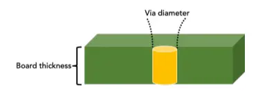
For designer engineers and printed circuit board (PCB) manufacturers alike, the concept of aspect ratio plays a crucial role in PCB functionality and manufacturability. Imagine a via as a straw connecting different layers of your PCB. The aspect ratio is like the ratio of the length of your straw to its diameter. Just like a long, thin straw can be difficult to work with, a high aspect ratio via presents challenges during the manufacturing process.
Challenges of a High Aspect Ratio
- Think of drilling a deep well with a narrow drill bit. The deeper you go, the more the drill bit can wander, potentially causing misaligned or damaged vias. Similarly, high aspect ratio vias require precise drilling techniques to maintain accuracy and prevent reliability issues.
- Electroplating challenges: Imagine filling a long, thin tube with liquid. Electroplating, the process of building up copper around the via walls for electrical connections between layers of a PCB, becomes more complex with high aspect ratios. Pushing the plating chemicals through a narrow hole and ultimately inspecting the plating in the hole are both challenging. Incomplete plating can lead to weak connections and potential electrical failures.
Why Consider Lower Aspect Ratio?
From a designer engineer’s perspective, adopting a lower aspect ratio whenever possible is a best practice for Design for Manufacturability (DFM). This translates to more robust and reliable PCBs for the board assembly process. Think of it as designing with the limitations of the manufacturing process in mind, ensuring a smooth and efficient production run.
Maximizing Space with Higher Aspect Ratio (when necessary)
There are situations where a higher aspect ratio can be beneficial. For complex and dense PCB designs, maximizing available board space for components and traces is paramount. A higher aspect ratio can be strategically employed to accommodate more vias within a limited area through reduction of via hole sizes and also the annular ring widths.
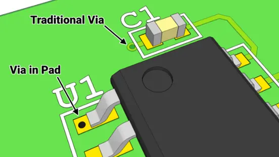
Via-in-Pad Technology: A Space-Saving Hero
Thankfully, innovative technologies like via-in-pad come to the rescue. Imagine placing the via right under the solder pad of a component, eliminating the need for dedicated via holes. This ingenious technique reduces the overall aspect ratio while still providing electrical connections, allowing for more efficient use of board space. There needs to be consideration for filling via-in-pad holes to prevent scavenging of solder from component joints. Via filling is a difficult process for high aspect ratio designs due to challenges of pushing the filling material into the smaller holes. Utilizing larger holes for via-in-pad with filled vias would be a good strategy. An equally valid strategy is to use smaller hole diameters for via-in-pad without filling if the pad area to hole size is kept at a high ratio.
Conclusion
Understanding aspect ratio empowers both designer engineers and manufacturers to create high-performance PCBs. While lower aspect ratios are generally preferred for manufacturability, a higher ratio can be strategically used in dense designs. By employing via-in-pad technology and keeping DFM principles in mind, we can achieve optimal designs that are compact, functional and manufacturable. If you have any design related questions around aspect ratios, via-in-pad, or any other PCB design practices, please contact us at info@canadiancircuits.com.